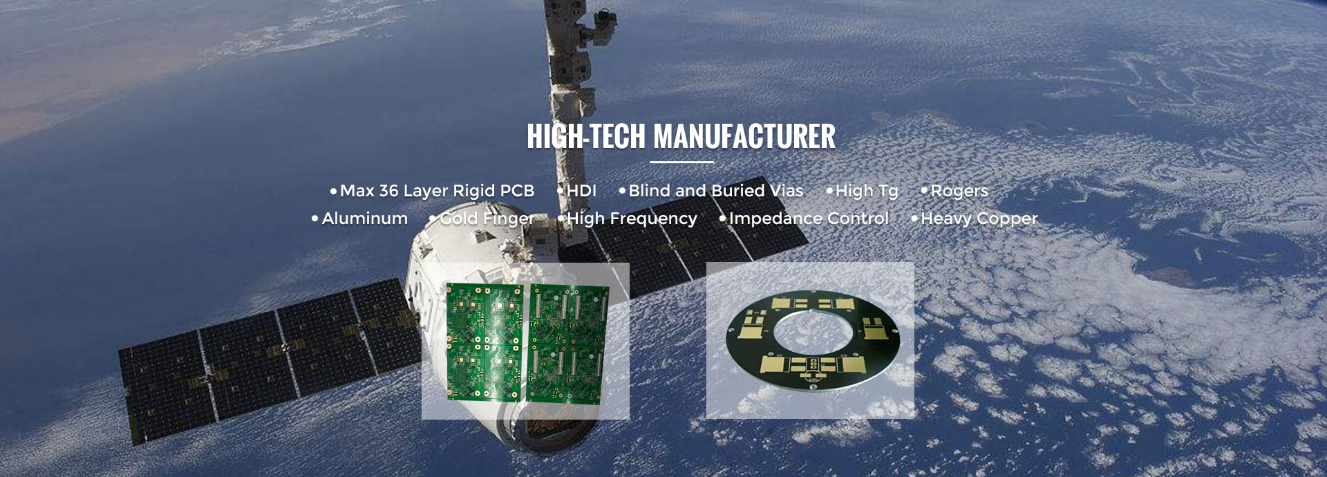
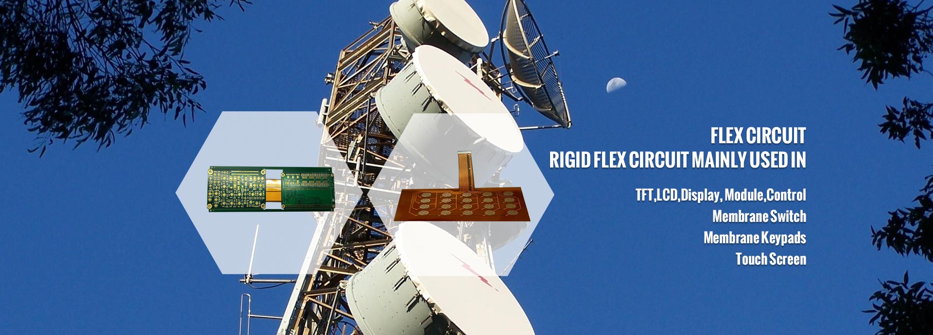
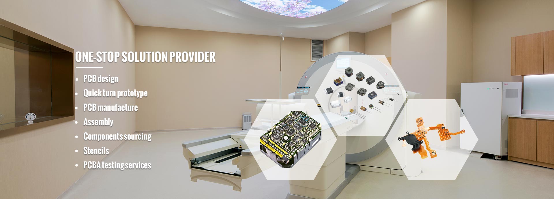
Dear Partners, welcome to MINKINZI – China’s Trusted End-to-End Manufacturing Partner, with 20 years of expertise, we specialize in: Design & Development → Max 58 Layer PCB Fabrication →Turnkey PCBA Assembly → Box-Build Assembly. ODM/OEM/Contract Manufacturing tailored to global standards. Support DFM. Welcome to send your NDA, PCB Gerber, BOM, so that we can provide quotation for you. .

  • High-Precision Probe Interface Board PCBA | Custom Test & Measurement Assembly

  • High-Precision Probe Interface Board PCBA | Custom Test & Measurement Assembly

  • High-Precision Probe Interface Board PCBA | Custom Test & Measurement Assembly

  • High-Precision Probe Interface Board PCBA | Custom Test & Measurement Assembly

  • High-Precision Probe Interface Board PCBA | Custom Test & Measurement Assembly

  • High-Precision Probe Interface Board PCBA | Custom Test & Measurement Assembly

High-Precision Probe Interface Board PCBA | Custom Test & Measurement Assembly

1. Semiconductor Test Probe Interface Board PCBA

2. PCB In-Circuit Test (ICT) Probe Interface Board PCBA

3. Flying Probe Test Interface Board PCBA

4. High-Speed Digital Probe Interface Board PCBA

5. RF & Microwave Probe Interface Board PCBA

6. MEMS Probe Interface Board PCBA

Share

Description :

Probe Interface Board PCBA – Professional Probe Interface Board PCBA Solutions

I. Overview of Probe Interface Board PCBA

The Probe Interface Board PCBA serves as a core component in semiconductor testing equipment, primarily functioning to connect and transmit signals between Automatic Test Equipment (ATE) and the Device Under Test (DUT). It establishes reliable electrical contact with wafers or packaged chips through precision probes or sockets, enabling the input, output, and feedback of test signals with exceptional accuracy.

Core Functions

A professionally engineered High-Precision Probe Interface Board delivers stable, low-loss electrical connections between the tester and the chip, while converting the tester's standardized interface into specialized configurations compatible with various chip packages. Through advanced Impedance-Controlled Probe Board design principles, it ensures superior Signal Integrity Probe PCBA performance during high-frequency transmission, effectively minimizing signal distortion. The architecture supports multi-channel parallel testing for enhanced throughput and incorporates a replaceable probe card design that simplifies maintenance, upgrades, and reduces overall testing costs.

Key Application Areas

The versatility of Multi-Layer Probe Interface Board solutions makes them indispensable across multiple semiconductor testing domains:

  • Semiconductor Wafer Testing (CP – Chip Probing)

  • Post-packaging Final Testing (FT – Final Test)

  • RF Chip Testing including 5G, Wi-Fi, and Bluetooth chips

  • SoC and MCU Testing

  • Memory Chip Testing covering DRAM and NAND Flash

  • Automotive Electronic Chip Testing (AEC-Q100 certification-related)

  • AI Chip and High-Performance Computing (HPC) Chip Testing


II. Probe Interface Board PCBA Key Technical Specifications

Technical ParameterTypical Specification
Layer CountRanging from 4-Layer Probe Interface Board to 20 layers, with 6-Layer Probe Interface PCB Assembly commonly deployed for mid-range applications and high-layer configurations exceeding 20 layers reserved for high-frequency requirements
Base MaterialHigh-Tg FR4, PTFE (Rogers, Taconic), Polyimide
Trace Width/SpacingStarting from 3 mil / 3 mil for High-Density Probe Interface PCB layouts
Impedance Control±5% precise matching engineered into every Impedance-Controlled Probe Board
Hole DiameterMechanical drilling ≥0.15mm; Laser drilling ≥0.075mm
Surface FinishENIG, Immersion Gold, Immersion Silver, OSP, Hard Gold
Operating FrequencyDC to 67 GHz, supporting High-Frequency Probe Interface PCBA and mmWave applications
Operating Temperature-55°C to +150°C
Noise PerformanceOptimized as a Low-Noise Probe Interface Board with integrated EMI Shielded Probe Interface Board architectures

III. Probe Interface Board PCBA Manufacturing Process Flow

PCB Manufacturing Stage

The fabrication of a High-Speed Probe Interface PCBA begins with high-precision pattern transfer and exposure, followed by vacuum etching and AOI inspection. Impedance testing and TDR verification ensure every Impedance-Controlled Probe Board meets stringent signal integrity requirements before multilayer lamination and precision drilling complete the foundation.

Component Procurement and Inspection

Strict BOM verification protocols are enforced, with procurement conducted exclusively through original manufacturer channels. Incoming Quality Control (IQC) inspection utilizing X-Ray and microscopy guarantees component authenticity and reliability.

SMT Assembly

Solder paste printing with SPI inspection initiates the assembly process, followed by high-speed placement supporting components as small as 0201. Dual inspection through AOI and X-Ray verification ensures placement accuracy, particularly critical for fine-pitch BGA and QFN packages in any High-Density Probe Interface PCB project.

Post-soldering & Conformal Coating

Selective wave soldering, conformal coating, and potting protect the assembly against environmental stresses. For Rigid-Flex Probe Interface PCBA designs, specialized handling procedures preserve the integrity of flexible sections.

Testing & Reliability Verification

Every Signal Integrity Probe PCBA undergoes flying probe testing, functional circuit testing (FCT), burn-in testing, thermal cycling from -40°C to +85°C, and comprehensive signal integrity validation before shipment.


IV. How to Choose Partners for Probe Interface Board PCBA

Selecting an EMS (Electronics Manufacturing Services) Provider

When evaluating EMS partners for your High-Precision Probe Interface Board requirements, prioritize providers with demonstrated experience in semiconductor test equipment and probe board projects. The ideal partner should support high-precision SMT and fine-pitch BGA/QFN packaging while maintaining quality systems certified to ISO 9001, IATF 16949, and AS9100 standards. Robust supply chain management with traceable component sourcing, comprehensive DFM (Design for Manufacturability) support, and streamlined NPI (New Product Introduction) processes are equally essential. Responsiveness in prototyping turnaround, mass production delivery, and flexible scheduling often distinguishes exceptional partners from average ones.

Selecting a PCB Manufacturer

The unique demands of High-Frequency Probe Interface PCBA manufacturing require a PCB manufacturer with deep expertise in high-frequency materials such as Rogers 4350B, Rogers 4003C, and Taconic substrates. The manufacturer must demonstrate impedance control capabilities with TDR testing equipment maintaining tolerances within ±5%, alongside high-layer-count manufacturing proficiency for complex boards exceeding 12 layers. Fine-line capabilities supporting stable mass production at 3mil/3mil line width/spacing are critical for any High-Density Probe Interface PCB application. Essential quality certifications include UL, IPC-A-600 Class 3, and IATF 16949, complemented by responsive engineering support, competitive sample lead times, and reliable after-sales service.

Selecting a Contract Manufacturer (OEM/ODM)

Technical compatibility with your product type and industry standards forms the foundation of a successful OEM/ODM partnership. Evaluate the manufacturer's production line configuration, including the number of SMT lines, placement accuracy, and inspection equipment capabilities (AOI, X-Ray, ICT). Production flexibility spanning small-batch pilot runs to large-scale mass production ensures scalability as your needs evolve. Confidentiality safeguards through rigorous NDA signing processes and information security mechanisms protect proprietary designs, while geographic location influences communication convenience, factory audit accessibility, and logistics efficiency. Transparent pricing structures with no hidden fees enable accurate cost forecasting.

Selecting a Turnkey PCBA Manufacturer

The turnkey model—encompassing manufacturing plus material sourcing—delivers the most streamlined partnership experience for Low-Noise Probe Interface Board clients. A qualified turnkey provider offers one-stop service covering PCB fabrication, component sourcing, SMT, assembly, and testing. Authorized manufacturer sources, distribution channels, and in-stock inventory capabilities mitigate supply chain risks. Proactive BOM risk management with End-of-Life (EOL) alerts and substitute recommendations prevents production disruptions. Cost advantages emerge from bulk purchasing power and economies of scale, while professional project management teams track progress from initiation through delivery. Quality assurance is reinforced through 100% pre-shipment testing and complete quality data traceability.


V. Why Global Clients Choose Minkinzi

Minkinzi brings extensive project experience in Probe Interface Board PCBA manufacturing, providing global clients with comprehensive one-stop solutions spanning design support, PCB manufacturing, component sourcing, SMT assembly, and final assembly and testing.Emailsales@minkinzi.com

Applications :

Minkinzi: Professional Manufacturing Solutions for Probe Interface Board PCBAs – A Factory Selection Guide for Semiconductor Test Equipment Customers

I. Core Application Areas for Probe Interface Board PCBAs

As the critical link between the tester and the Device Under Test (DUT) in semiconductor Automated Test Equipment (ATE), Probe Interface Boards are widely deployed across a range of high-precision testing environments. As a trusted Probe Interface Board PCBA Manufacturer and Probe Interface Board PCBA Supplier, Minkinzi delivers solutions tailored to the most demanding semiconductor test applications:

  • Wafer Testing (CP – Chip Probing): Connecting the probe card to the tester to perform electrical performance testing at the wafer level.

  • Final Testing (FT): Connecting the test socket to the ATE to verify the functionality of packaged chips.

  • RF/Millimeter-Wave Testing: Signal integrity testing platforms for 5G, Wi-Fi 6/7, and millimeter-wave devices.

  • Automotive-Grade Chip Testing: High-reliability testing for AEC-Q100 certified chips.

  • High-End SoC/AI Chip Testing: Testing for chips with high pin counts and high data rates (e.g., PCIe 5.0/6.0, USB4, SerDes).


II. Manufacturing Challenges (Core Pain Points) for Probe Interface Board PCBAs

As an experienced Probe Interface PCBA China Supplier, Minkinzi understands the intricate technical challenges involved in producing high-performance Probe Interface Board PCBAs. The following table summarizes the core manufacturing pain points we address daily:

Challenge CategorySpecific Technical Challenges
High-Frequency Signal IntegrityMust support GHz-level signal transmission; extremely strict requirements for impedance control (±5% or even ±3%), insertion loss, and return loss.
High-Frequency Material SelectionUses high-frequency substrates such as Rogers RO4350B, RO4003C, PTFE, and Isola; complex mixed-lamination processes with FR-4.
High-Layer-Count StructureTypically 8–20 layers; strict requirements for stack-up symmetry and Z-axis Coefficient of Thermal Expansion (CTE) control.
High-Density Interconnect (HDI)Fine circuitry (3mil/3mil), micro-vias/blind & buried vias (HDI Any-layer), BGA/PGA packaging.
Gold Finger/Contact ReliabilityGold plating thickness (options of 30μ" or 50μ"), nickel layer density, and high durability requirements for mating cycles.
Impedance Matching PrecisionStrict matching (e.g., 100Ω differential, 50Ω single-ended); TDR testing must meet design specifications.
Thermal DesignPCB thermal resistance control for high-current testing scenarios; metal substrate or embedded copper block structures.
DFM/DFT CollaborationHighly customized mechanical and electrical interfaces for ATE systems and probe cards.

III. Checklist of Core Customer Requirements for PCB/PCBA Manufacturers

When customers search for the Best Probe Interface Board PCBA provider, they typically evaluate manufacturers against the following comprehensive criteria. At Minkinzi, we meet and exceed each of these benchmarks.

Technical Capability Requirements

  • Comprehensive High-Frequency Material Portfolio: Stocking capabilities for Rogers, Isola, and Shengyi high-frequency laminates; mature mixed-lamination processes.

  • Impedance Design Capabilities: SI simulation, stack-up design, and TDR test report generation.

  • HDI and Micro-via Processes: Laser drilling, via-filling plating, and Any-layer interconnection capabilities.

  • High-Layer-Count Board Processes: Alignment control (±0.05mm) for 12, 16, and 20-layer boards.

  • Specialized Process Capabilities: Back-drilling, stepped gold fingers, depth-controlled drilling, embedded copper blocks.

Quality Control Requirements

  • Incoming Quality Control (IQC): Batch traceability for high-frequency materials; testing of Tg, Df, and dielectric constant (Dk).

  • In-Process Quality Control (IPQC): AOI, impedance testing, and XRF sampling for plating thickness.

  • Outgoing Quality Control (OQC):

    • 100% Flying Probe/ICT testing

    • TDR impedance test reports

    • Metallographic cross-sectioning for gold plating thickness

    • Solder joint inspection via X-ray/AOI

    • High-frequency S-parameter testing (optional)

  • System Certifications: ISO 9001, ISO 14001, IATF 16949 (required for automotive clients)

  • Reliability Testing: Thermal shock (-55°C to 125°C), aging tests, and mating cycle/durability verification.

Delivery Capability Requirements

  • Rapid Prototyping: Expedited prototyping for small batches (5–20 pcs) completed in 5–7 days.

  • Stable Mass Production Lead Times: Standard lead time of 15–20 working days; 20–25 days for HDI/High-Frequency boards.

  • Flexible Production Capacity: Seamless transition from NPI-stage high-mix/low-volume production to mass production ramp-up.

  • Progress Visibility: Online work order system with real-time feedback on key milestones.

  • Global Logistics: Support for DDP/DAP terms; 3–5 day delivery to key customer regions.

  • Inventory Management (VMI): Safety stock management services available for strategic customers.

Engineering Support Requirements

  • DFM (Design for Manufacturability) Review: DFM reports issued within 48 hours.

  • SI/PI Simulation Support: Collaborative signal integrity optimization with customers.

  • Failure Analysis (FA): Rapid response via 8D reports, including root cause analysis and corrective actions.

  • Alternative Material Solutions: Recommendations for equivalent-grade material substitutions to address shortages or reduce costs.

Commercial and Confidentiality Requirements

  • NDA Process: Support for rapid signing of one-way or mutual non-disclosure agreements.

  • IP Protection: Encrypted storage and access control for customer drawings and Gerber files.

  • Dedicated Production Lines: Exclusive production units available for high-security projects.

  • Flexible Payment Terms: Support for various settlement methods, including credit terms, L/C, and T/T.


IV. Our Differentiated Advantages

When global buyers seek to Buy Probe Interface Board PCBA Online or partner with a dependable Probe Interface Board PCBA Factory, Minkinzi stands apart through our specialized expertise and proven capabilities.

Focus on the Semiconductor Testing Sector

With over a decade of deep specialization in the niche markets of Probe Interface Boards, Load Boards, and Probe Card PCBs, we have served a cumulative total of hundreds of clients across ATE equipment manufacturers, OSATs, and IDMs. Our Custom Probe Interface Board PCBA Service model allows us to adapt to the unique requirements of each customer, regardless of project complexity.

High-Frequency & High-Speed Process Platform

Our state-of-the-art facility is equipped with advanced machinery including LDI (Laser Direct Imaging), vacuum presses, and depth-controlled drilling systems. We deliver:

  • Impedance control precision of ±5%

  • TDR test first-pass yield greater than 98%

  • Support for up to 20 layers and 4+N+4 HDI structures

As a leading High-Frequency PCB Impedance Control Factory, we ensure that every board meets the most stringent signal integrity requirements demanded by today's high-speed semiconductor devices.

Rigorous Quality System

Quality is embedded in every step of our process. As a High-Quality Probe Interface PCBA provider, we implement:

  • Full-process MES traceability system with QR code tracking for individual boards throughout their lifecycle

  • Process capability control with CPK ≥ 1.67 for critical processes

  • Comprehensive compliance documentation (PPAP, CPK, MSDS, RoHS, REACH)

Flexible Manufacturing & OEM/ODM Services

Whether you require OEM Probe Interface Board Assembly or full-scale ODM Probe Interface PCBA development, our engineering team is ready to collaborate. We support:

  • Wholesale Probe Interface Board PCBA orders with scalable production capacity

  • Affordable Probe Interface Board Assembly solutions without compromising quality

  • End-to-end turnkey services from design review to global delivery


V. Comprehensive Product Portfolio

Core ProductSpecialized Service
Probe Interface Board PCBASemiconductor Test Board PCBA Manufacturer
Load Board PCBAHigh-Frequency PCB Impedance Control Factory
Probe Interface Board SMTRogers Material Hybrid-Laminate PCB Manufacturer
ATE Test Board PCBA20-Layer High-Frequency Board PCBA Turnkey Service
Probe Card PCB AssemblyHDI (High-Density Interconnect) Board Manufacturer
Semiconductor Test Fixture PCBAGold-Finger Plating PCB Factory

Get in Touch

Whether you are an ATE equipment manufacturer, an OSAT provider, or an IDM looking for the Best Probe Interface Board PCBA partner, Minkinzi is your trusted choice for reliability, precision, and performance.

Contact Minkinzi today for Probe Interface Board PCBA manufacturing solutions tailored to your exact needs.Emailsales@minkinzi.com

Flow Chart :

Comprehensive Overview of the Probe Interface Board PCBA Process: Minkinzi's Workflow from Prototype Validation to Mass Production

In the field of precision testing equipment, the Probe Interface Board serves as the critical link between testing instruments and the Device Under Test (DUT). Its performance directly determines the accuracy and stability of test data. From the initial schematic to the stable supply of tens of thousands of units, rigorous end-to-end PCBA process control is the cornerstone of product reliability. As a trusted partner for Turnkey Probe Interface Board PCBA, Minkinzi delivers an integrated, one-stop service model that helps global customers accelerate time-to-market while reducing total cost of ownership.


Requirements Alignment and Solution Evaluation (1–3 Working Days)

Customer Requirement Confirmation

The journey begins with a thorough collection of technical documentation, including Gerber files, BOM (Bill of Materials), schematics, 3D structural files, and test specifications. Our engineering team invests time in understanding the application scenario—because Probe Interface Boards are typically deployed in IC test sockets, ATE (Automatic Test Equipment), and wafer probers, key parameters such as impedance, signal integrity, and mating cycle lifespan must be clearly defined. Special processes are also identified upfront, including gold finger thickness, ENIG/Immersion Silver finishes, impedance matching control, and high-frequency material selection (such as Rogers and FR-4 high-frequency hybrid laminates). This is a foundational step in our One-Stop Probe Interface PCBA Service, ensuring that every downstream activity is aligned with the customer's real-world application.

DFM (Design for Manufacturability) Review

A team of professional engineers conducts twelve manufacturability checks on the design files, covering minimum trace width and spacing (typically ≥3 mil) relative to process capabilities, adequacy of solder mask dams and pad spacing, solder mask opening designs for BGA and QFN components, matching of stencil apertures to solder paste volume, and test point coverage. This proactive DFM review is embedded in our Probe Interface PCB Fabrication and Assembly workflow to eliminate design risks before production begins.

Quotation and Lead Time Confirmation

We provide transparent itemized quoting covering bare PCB, materials, SMT, testing, and assembly, with tiered pricing options to facilitate mass production cost evaluation. Clear commitment to lead times is paired with proactive identification of potential risks—principles that have made our Turnkey Probe Interface Board PCBA offering a preferred choice for global OEMs.


Prototype Stage: 5–10 Working Days

The prototype stage is a critical phase for validating design and process feasibility, requiring speed, accuracy, and stability. As specialists in Prototype Probe Interface Board PCBA, we compress the learning curve while protecting design integrity.

Bare PCB Manufacturing

Material selection is driven by customer requirements, with options including FR-4, high-frequency boards, and aluminum-based boards. Precision control of multi-layer board lamination and laser drilling (aperture ≥0.1mm) ensures mechanical and electrical accuracy. Surface finishes such as ENIG (Electroless Nickel/Immersion Gold), Immersion Tin, OSP, and Immersion Silver are applied based on use case—ENIG is most commonly selected for probe boards to guarantee contact reliability and oxidation resistance. Impedance control is verified through 100% testing of differential and single-ended lines using impedance testers, a key value-add in our Probe Interface PCB Fabrication and Assembly capability.

Component Procurement

All components are sourced through authorized channels—original manufacturer-authorized agents or Tier-1 distributors—with strict avoidance of refurbished or loose/un-reeled parts. Incoming Quality Control (IQC) performs batch sampling of critical ICs, connectors, and special materials listed in the BOM. Shortage alerts are escalated immediately, with alternative component solutions proposed to keep prototypes on schedule.

SMT Assembly & DIP Insertion

Our SMT Assembly Probe Interface Board capability begins with fully automatic solder paste printers combined with SPI (Solder Paste Inspection) systems to control paste thickness and volume. High-precision placement machines (such as Yamaha YSM and Fuji NXT) support components as small as 01005 alongside odd-form parts. Reflow soldering is performed under nitrogen protection with precise temperature profile control, with peak temperature maintained at 245±5°C for lead-free processes. For components requiring Through-Hole Probe Interface Assembly, we apply wave soldering or selective wave soldering—an essential capability for the large connectors typically found on probe boards. This combination of surface-mount and through-hole processes defines our Mixed Technology Probe Interface PCBA expertise.

Sample Quality Inspection

Quality verification is multi-layered. AOI (Automated Optical Inspection) provides 100% inspection before and after reflow to detect cold joints, solder bridges, and tombstones. X-Ray inspection performs transmission analysis for components with hidden bottom-side solder joints, such as BGAs and QFNs. First Article Inspection (FAI) verifies dimensions, polarity, and silkscreen markings against design files. Functional Testing (FCT) is conducted using test fixtures constructed based on customer test plans to verify electrical performance.

Sample Delivery and Improvement

Customers receive comprehensive test reports, including AOI reports, X-ray images, and ICT/FCT data. Our engineering team collaborates with the customer on design optimization recommendations covering thermal management, EMI shielding, and trace routing improvements. A sample Bill of Materials is compiled to prepare for bulk material procurement, ensuring a seamless transition to the next stage.


Pilot Run Stage: The "Touchstone" for Process Validation

Successful sample validation does not lead directly to mass production. The pilot run, typically involving 50–500 units, serves as a critical bridge and is a core offering within our Low-Volume Probe Interface Board Assembly service. This stage is where the real-world stability of the process is proven.

Trial Production Objectives

The pilot run verifies the stability and yield of the mass production process, identifies potential issues in material compatibility, stencil design, and test coverage, optimizes production cycle time and staffing allocation, and finalizes process parameters and work instructions for formal mass production.

Trial Production Control Points

A pre-production meeting (PRE) brings together Engineering, Quality, Production, and Planning for a joint review. First-article confirmation is required before mass production proceeds, with sign-off from both the Quality Department and the customer. In-process quality control (IPQC) monitors quality using AQL sampling standards, while data collection includes CpK process capability analysis to ensure capability indices for critical processes reach ≥1.33.

Reliability Testing (Optional)

To meet the high-reliability requirements of probe interface boards, the following tests may be conducted: temperature and humidity cycling test (-40°C to +85°C), vibration and shock testing, mating cycle/durability test simulating repeated use of the probe board, insulation withstand voltage test (Hi-Pot Test), and salt spray test for applications in special environments.


Mass Production: Capability for Stable Delivery

When the pilot run is approved, the project transitions into our Mass Production Probe Interface PCBA program, designed for predictable output, consistent quality, and on-time delivery at scale.

Production Preparation

Material completeness is verified with 100% receipt of all BOM materials under FIFO inventory management. Tooling and fixture preparation ensures that test fixtures, programming fixtures, and packaging trays are ready before the first unit is built. Production scheduling is built around customer delivery dates, with daily/weekly capacity planning and buffers allocated for critical processes.

Mass Production Process

Process StepEquipment / MethodKey Control Points
Solder Paste PrintingFully automatic printer + SPISolder paste thickness, volume, offset
Component PlacementHigh-speed mounterPlacement accuracy, feeder status
Reflow SolderingNitrogen reflow ovenTemperature profile, solder quality
AOI Inspection3D AOISolder joint morphology, component polarity
X-RayIndustrial X-RayBGA void ratio, bridging
ICT TestingIn-Circuit TesterOpen/short circuits, component values
FCT (Functional Circuit Test)Customer-specified schemeElectrical performance, functional specifications
Conformal CoatingSpraying / dippingCoating uniformity, coverage integrity
Burn-in TestConstant-temperature burn-in chamberEarly failure screening
Packaging & ShipmentAnti-static packagingLabeling, protection, traceability

Conclusion: Ensuring Every Probe Interface Board Stands the Test of Quality

From the first DFM review to the final packaged shipment, Minkinzi delivers a seamless, end-to-end Probe Interface PCB Fabrication and Assembly experience. Whether you need a fast Prototype Probe Interface Board PCBA build, a tightly controlled Low-Volume Probe Interface Board Assembly pilot, scalable Mass Production Probe Interface PCBA, or a fully integrated Turnkey Box Build for Probe Interface Board, our engineering depth, manufacturing capacity, and quality discipline are built to protect your test integrity.

Welcome to contact Minkinzi to manufacture your Probe Interface Board PCBA.Emailsales@minkinzi.com

Capability :

Minkinzi — Your Trusted One-Stop Partner for Probe Interface Board PCBA Manufacturing (Turnkey Service)

Leading Probe Interface Board PCBA Manufacturer with Full Turnkey Capabilities

Minkinzi is a specialized one-stop electronics manufacturing service provider focused on high-end PCB fabrication, full-turnkey PCBA manufacturing, and the precision production of Probe Interface Boards. With years of deep expertise in high-precision sectors—including test fixture boards, probe card interface boards, ATE load boards, and IC test boards—Minkinzi delivers comprehensive, end-to-end solutions that cover every stage of production, from PCB lamination and SMT assembly to DIP insertion, BGA reballing, conformal coating, and full-board testing. Our integrated approach to PCB Layout for Probe Interface Board design and manufacturing ensures that every project is optimized for signal integrity, mechanical stability, and long-term reliability in demanding test environments.


Probe Interface Board PCBA Manufacturing Capabilities (Key Parameters)

Our advanced manufacturing capabilities enable us to serve the most demanding Test & Measurement Probe Interface Board applications across global industries:

ItemCapability Parameter
PCB Layer Count2–30 layers (supports blind/buried vias, HDI Any-layer)
Board Thickness0.2mm – 6.0mm
Min. Line Width/Spacing2.5mil / 2.5mil (high-end: 2mil/2mil)
Min. Hole DiameterMechanical drilling: 4mil; Laser drilling: 2mil
Impedance Control±5% (high-end: ±3%)
MaterialsFR4, High-Tg, Microwave, Taconic, Nelco, Arlon, PTFE
Surface FinishENIG, ENEPIG, OSP, Immersion Gold, Immersion Tin, Immersion Silver, Hard Gold
Copper ThicknessInner layers: 1oz–6oz; Outer layers: 1oz–12oz
BGA PitchMin. 0.25mm pitch
Min. Package Size01005, 0.3mm pitch CSP

SMT and PCBA Manufacturing Capabilities

Minkinzi's SMT lines are built for the precision required in Component Sourcing Probe Interface PCBA and high-density assembly:

  • Placement Accuracy: ±0.025mm (Cpk ≥ 1.67)

  • Placement Speed: >80,000 CPH per unit; multi-line parallel processing

  • Component Range: 01005 to large BGA, QFN, PoP, and odd-form components

  • Reflow Soldering: Nitrogen-protected reflow; 12-zone adjustable temperature profile

  • AOI / X-Ray / ICT / FCT: 100% full inspection + in-line testing

  • BGA Rework: Professional BGA reballing and rework stations

  • Conformal Coating / Potting: Selective coating, UV curing, precision dispensing

  • Special Processes for Probe Interface Boards: High-flatness depth control (≤0.05mm), high-durability ENIG finish, thickened plating for micro-vias, impedance matching testing


Production and Delivery Capabilities

Minkinzi combines scalable capacity with rapid-turn execution to support both prototyping and mass production:

  • Bare PCB Monthly Capacity: 80,000 m²

  • PCBA Monthly Capacity: Over 5 million placement points (SMT)

  • Rapid Prototyping: PCB (24–72 hour rush service), PCBA (3–5 days)

  • Mass Production Lead Time: Standard 7–10 days; rush service 5–7 days

  • Multi-Project Management: Capable of managing 200+ active projects simultaneously

  • Global Delivery: Supports DHL/FedEx, sea/air freight; flexible trade terms (DDP/DAP)


Supply Chain & Turnkey Manufacturing Advantages

Our robust Component Sourcing Probe Interface PCBA infrastructure eliminates supply chain risk and accelerates time-to-market:

  • Authorized Component Channels: Direct partnerships with manufacturers and Tier-1 distributors (e.g., TI, ADI, Maxim, Murata, TDK)

  • BOM Sourcing Accuracy: ≥99.8%; alternative part recommendations provided within 24 hours for shortages

  • BOM Cost Optimization: Domestic/import substitution options available to save 10%–30% on costs

  • Long Lead-Time Material Alerts: 3-month advance warnings; strategic stock maintained for critical components

  • Strategic PCB Material Inventory: Stocking high-end materials (e.g., Rogers, Taconic) for high-frequency and high-speed boards

  • Shortage / EOL Materials: Dedicated End-of-Life solutions and a global sourcing network


Pricing Advantages

Minkinzi delivers exceptional value through factory-direct efficiency and engineering-driven cost control:

  • Factory-Direct Operations: No middleman markups; prices 8%–15% lower than market averages

  • Free Engineering Optimization: Complimentary DFM checks, stack-up optimization, and alternative component solutions

  • Tiered Pricing: Annual framework agreement pricing for long-term partners

  • All-in-One Turnkey Pricing: Saves over 20% in logistics and time costs compared to separate procurement


Quality Control System

Quality is engineered into every step of our Probe Interface Board PCBA workflow:

  • System Certifications: ISO 9001, ISO 14001, IATF 16949, UL, RoHS, REACH

  • Testing Equipment: Flying probe tester, impedance tester, cross-section microscope, X-Ray, SPI, AOI, ICT, FCT, thermal cycling chamber

  • Quality Standards: IPC-A-600, IPC-A-610 Class 2/3, IPC-6012 Class 3

  • Yield Control: PCBA first-pass yield ≥99.5%

  • Traceability: Full barcode traceability for every component, board material batch, and process step; data retained for over 5 years


Industry Applications & Typical Probe Interface Board Case Studies

Minkinzi has delivered over 300 probe interface board projects across multiple high-reliability industries. Our cross-sector expertise allows us to tailor solutions for the unique electrical, mechanical, and regulatory demands of each application.

Automotive Probe Interface Board PCBA Contract manufacturing of 16-layer high-speed test boards for an IC design company; impedance tolerance ±5%; over 50,000 units delivered in mass production. Our IATF 16949-certified Automotive Probe Interface Board PCBA solutions are supplied to multiple domestic Tier 1 suppliers for automotive MCU probe testing, ensuring compliance with the strictest automotive quality standards.

Telecommunications Probe Interface PCBA We provide high-frequency, high-speed Telecommunications Probe Interface PCBA solutions for 5G RF probe stations and base station test systems. Utilizing Taconic and Arlon high-frequency materials with dielectric constant (Dk) tolerance of ±0.05, our boards support the most demanding telecom test applications.

Aerospace Probe Interface Board Assembly Minkinzi's Aerospace Probe Interface Board Assembly services are GJB (military standard) certified, with multiple products in stable, long-term operation. We serve defense and aerospace customers who require the highest reliability under extreme environmental conditions.

Medical Device Probe Interface PCBA Our Medical Device Probe Interface PCBA solutions are CE/UL certified and used in CT scanners, ultrasound systems, and other medical imaging equipment probe connections. We understand the regulatory landscape and deliver boards that meet medical-grade reliability and traceability requirements.

Industrial Automation Probe Interface Board For smart manufacturing and industrial test systems, our Industrial Automation Probe Interface Board products deliver robust performance in harsh factory environments, supporting high-volume production test of industrial sensors, controllers, and power modules.

Consumer Electronics Probe PCBA Minkinzi produces Consumer Electronics Probe PCBA solutions using rigid-flex board technology for mobile phone module testing and other high-volume consumer device applications, balancing cost efficiency with precision performance.

Test & Measurement Probe Interface Board Specializing in Test & Measurement Probe Interface Board manufacturing, we support GPU/CPU burn-in test fixture boards (8–12 layer HDI with over 3,000 test points), ATE load boards, and IC test boards for the global semiconductor test industry.

Laboratory Equipment Probe Interface PCBA Our Laboratory Equipment Probe Interface PCBA capabilities serve research institutions, diagnostic equipment manufacturers, and precision instrument producers who require highly customized, low-volume, high-mix probe interface solutions.

AI Chip Burn-in Boards Supporting AI computing chip manufacturers, we provide turnkey burn-in testing services covering both manufacturing and materials for next-generation AI accelerator validation.

LED Wafer Test Probe Card Interface Boards With high flatness (≤0.03mm), our LED wafer test probe card interface boards are currently in mass production delivery, supporting the LED semiconductor industry's stringent optical and electrical test requirements.

New Energy Battery BMS Test Boards High-voltage, high-current test boards certified for relevant safety standards, serving the rapidly growing new energy vehicle and energy storage markets.

Contact Minkinzi for Your Probe Interface Board PCBA Project

Whether you need Automotive Probe Interface Board PCBATelecommunications Probe Interface PCBAAerospace Probe Interface Board AssemblyMedical Device Probe Interface PCBAIndustrial Automation Probe Interface BoardConsumer Electronics Probe PCBATest & Measurement Probe Interface Board, or Laboratory Equipment Probe Interface PCBA, Minkinzi is your trusted manufacturing partner.

Emailsales@minkinzi.com

Advantages :

Minkinzi – Your Trusted Partner for High-Performance Probe Interface Board PCBA Manufacturing

Minkinzi is a globally recognized manufacturer specializing in the design, fabrication, and assembly of high-reliability Probe Interface Board PCBA solutions for the semiconductor test, ATE (Automatic Test Equipment), and advanced electronics industries. From initial Probe Interface Board Design consultation to full-scale production, SMT assembly, and rigorous functional verification, we deliver end-to-end Probe Interface PCB Assembly services that meet the most demanding signal integrity, mechanical precision, and cleanliness requirements of modern wafer probe testing and device validation applications.

Whether you require a Custom Probe Interface Board for a unique ATE platform, a high-density Probe Interface Module PCBA with ultra-fine pitch BGAs, a Probe Interface Control Board for instrument-level integration, or a high-speed Probe Signal Interface Board engineered for >10 Gbps data rates, Minkinzi provides the engineering depth, manufacturing capability, and quality systems to bring your project to life—on time, on spec, and at scale.


Core Manufacturing Advantages

Our vertically integrated production lines are purpose-built for the unique challenges of probe interface board manufacturing, where signal fidelity, dimensional precision, and long-term reliability are non-negotiable.

Advantage CategoryCapability Description
Special Material ProcessingExpert processing of high-frequency and high-speed base materials, including Rogers (RO4003C, RO4350B, RO3003), Taconic (TLX/TLY), Panasonic (MEGTRON 6 / MEGTRON 7), Isola (FR408HR, IS620), and Nelco laminates—ideal for any Probe Interface Circuit Board requiring low loss, low Dk, and tight dielectric tolerance.
Hybrid Lamination TechnologySupports hybrid stackups combining FR-4 with high-frequency materials, delivering both low-loss signal transmission and robust mechanical strength for rugged Probe Board Assembly applications.
Trace Width / SpacingMinimum trace width and spacing of 2.5 mil / 2.5 mil (63.5 μm), enabling high-density interconnect (HDI) routing essential for compact Probe Interface PCB layouts.
Layer Count CapabilityProduction capability for 4 to 58 layer boards, with symmetrical stackup design that preserves signal integrity across high-speed signal paths.
Impedance ControlTight impedance tolerance of ±5% (±3% on select specifications), verified with Polar Si8000 and InCoupon impedance testing systems—critical for Probe Signal Interface Board performance at multi-gigabit speeds.
Hole PrecisionMinimum laser drill diameter of 3 mil (0.075 mm), hole position accuracy of ±2 mil, and excellent plating uniformity on hole walls for reliable via performance.
HDI CapabilityFull support for 1+N+1, 2+N+2, and 3+N+3 any-layer HDI structures, with a mature any-layer interconnect process for complex Probe Interface Module PCBA designs.
Surface FinishComprehensive finish options including ENIG, ENEPIG, Immersion Gold, Immersion Silver, OSP, Hard Gold, and Soft Gold. Hard Gold and ENEPIG are most commonly specified for probe contact areas to maximize mating cycle durability.
Special ProcessesBack drilling, depth control drilling, cavity (stepped slot) machining, and press-fit hole preparation for advanced Custom Probe Interface Board architectures.

Inspection and Testing Capabilities

Quality assurance at Minkinzi is built on a foundation of best-in-class inspection and metrology equipment, covering every stage of Probe Interface Board PCBA production.

PCB Inspection Equipment

EquipmentPurpose
Flying Probe Tester / Open-Short Circuit TesterIdeal for small-batch, high-density probe card and Probe Interface Circuit Board validation.
Automated Optical Inspection (AOI)Detects visual defects including line width, spacing, pad geometry, and hole positioning.
X-Ray Inspection SystemNon-destructive verification of BGA solder joints, interlayer alignment, and hole wall quality.
Impedance Tester (Polar Si8000 + TDR)Characteristic impedance measurement and verification for high-speed signal paths.
Metallurgical MicroscopeCross-section analysis of barrel copper thickness, plating quality, and lamination integrity.
Micro-sectioning EquipmentPrecision preparation of PCB cross-section samples for reliability assessment.
2D / 3D Video Measuring SystemHigh-accuracy measurement of hole positions, diameters, and overall dimensions.
Thermal Stress Tester288 °C / 10 s / 3-cycle solder float test to verify barrel copper reliability.
Ionic Contamination TesterMeasures ionic residues on PCB surfaces—essential for probe-grade cleanliness.
Solderability TesterSolderability validation for all finished boards.
Breakdown Voltage TesterHigh-voltage insulation reliability verification.

PCBA Inspection Equipment

EquipmentPurpose
SMT Assembly LineYamaha / Fuji / Panasonic high-speed mounters supporting 01005 components and 0.4 mm pitch BGAs.
Reflow / Wave SolderingNitrogen-protected reflow soldering ensuring joint consistency and minimal voiding.
3D SPI (Solder Paste Inspection)Real-time solder paste printing quality control.
3D AOIPost-placement and post-reflow quality verification for every Probe Board Assembly.
X-Ray (2D / 3D CT)Inspection of hidden solder joints on BGA, QFN, and CSP packages.
ICT (In-Circuit Test) / FCT (Functional Test)Customer test program loading and full functional verification of the Probe Interface Control Board.
BGA Rework StationHigh-precision rework for BGA and QFN chips.
Ionic Cleanliness TesterControls ionic residues on assembled PCBAs to probe-grade levels.
Temperature & Humidity Cycling ChamberVerifies long-term reliability of the Probe Signal Interface Board under thermal cycling.
Boundary Scan Tester (JTAG)Validates complex digital interconnects on dense Probe Interface Module PCBA designs.

International Standards Compliance

Minkinzi's manufacturing processes and quality systems are aligned with the world's most respected electronics industry standards, giving procurement and engineering teams total confidence in every Probe Interface PCB Assembly shipment.

PCB Manufacturing Standards

StandardTitleScope
IPC-6012Qualification and Performance Specification for Rigid Printed BoardsGeneral quality benchmark for multilayer Probe Interface Circuit Board products.
IPC-6012 Class 3High-Reliability Electronic ProductsRecommended classification for high-reliability probe boards.
IPC-6013Qualification and Performance Specification for Flexible Printed BoardsFlexible Probe Interface PCB applications.
IPC-A-600Acceptability of Printed BoardsVisual acceptance criteria.
IPC-2221 / 2222Generic / Rigid PCB Design StandardsDesign guidelines for manufacturability.
IPC-4101Specification for Base Materials for Rigid and Multilayer Printed BoardsMaterial specifications.
IPC-4552ENIG SpecificationElectroless Nickel / Immersion Gold process standard.
IPC-4556ENEPIG SpecificationElectroless Nickel / Electroless Palladium / Immersion Gold—preferred for probe contact durability.
UL 796Standard for Safety for Printed-Wiring BoardsFlame retardancy and electrical safety.

PCBA Manufacturing Standards

StandardTitleScope
IPC-A-610Acceptability of Electronic AssembliesCore acceptance standard for Probe Board Assembly (Class 3 recommended).
IPC-7711 / 7721Rework, Modification and Repair of Electronic AssembliesRework process specifications.
IPC-J-STD-001Requirements for Soldered Electrical and Electronic AssembliesSoldering process requirements.
IPC-9191General Requirements for Implementation of Statistical Process Control (SPC)Process control and continuous improvement.
IPC-CC-830Qualification and Performance of Electrical Insulating Compound for Printed Board AssembliesConformal coating application.
IPC-SM-785SMT Soldering Accelerated Reliability TestingReliability verification methodology.

Quality Management System Standards

StandardTitle
ISO 9001:2015Quality Management Systems
ISO 14001:2015Environmental Management Systems
IATF 16949:2016Automotive Quality Management Systems (where automotive-grade applies)
ISO 13485:2016Medical Devices – Quality Management Systems (where medical-grade applies)
AS9100DAerospace Quality Management Systems (where aerospace-grade applies)
IEC 61340Electrostatic Discharge (ESD) Protection Standards
ANSI/ESD S20.20ESD Control Program Certification

Why Leading ATE OEMs Choose Minkinzi for Probe Interface Board PCBA

High-Frequency Signal Integrity Expertise – End-to-end capabilities covering material selection, electromagnetic simulation, stack-up design, and final test verification ensure that every Probe Signal Interface Board we deliver meets the strictest signal integrity targets.

Ultra-Low-Loss Material Inventory – Ready stock of Rogers, Taconic, and Panasonic high-frequency laminates dramatically shortens lead times for critical Custom Probe Interface Board programs.

Impedance Precision ±5% – Verified impedance control supports high-speed signal transmission exceeding 10 Gbps—essential for next-generation Probe Interface Module PCBA platforms.

ENEPIG Surface Finish – Wear-resistant, low-oxidation finish specifically selected for probe contact areas, capable of withstanding tens of thousands of mating cycles without degradation.

Probe-Grade Cleanliness Control – Ionic contamination maintained below 1.56 μg NaCl/in² (per IPC-TM-650 2.3.25), the standard required for reliable probe contact performance.

ATE Platform Experience – Deep familiarity with interface board design for mainstream ATE platforms including Teradyne, Advantest, and Cohu—reducing ramp-up time and engineering risk on your next Probe Interface Board Design.Contact our sales engineering team: Emailsales@minkinzi.com

Materials :

Minkinzi – Expert Manufacturer of Probe Interface Board PCBAs

Minkinzi is a trusted expert manufacturer of high-performance Probe Interface Board PCBAs, delivering complete PCB fabrication, advanced PCBA assembly, and one-stop turnkey services for semiconductor, IC testing, medical imaging, RF, and industrial applications. Our engineering team specializes in building reliable, signal-integrity-optimized solutions such as the Semiconductor Probe Interface BoardWafer Probe Interface PCBAProbe Card Interface Board AssemblyATE Probe Interface Board PCBAIC Testing Probe Interface BoardFlying Probe Interface PCBAMedical Probe Interface BoardUltrasound Probe Interface PCBAIndustrial Probe Interface Board, and RF Probe Interface Board Assembly — all designed to meet the strict demands of modern automated test and validation environments.


PCB Manufacturing Expertise (Categorized by Material and Structure)

High-Frequency / High-Speed Material PCBs

For RF Probe Interface Board Assembly and high-frequency signal test applications, Minkinzi fabricates PCBs using premium low-loss materials, including PTFE-based laminates such as Rogers RO4003C, RO4350B, and RO3003, Taconic TLX/TLY/TLC series, and Isola I-Tera MT40. We also work with advanced low-loss high-speed materials such as Mitsubishi CCL-HL832, Panasonic MEGTRON 6/7, and TU-872 SLK. These materials are ideal for high-frequency probe interface boards, 5G/RF test boards, and high-speed digital test interface boards where signal integrity is critical.

Specialty FR-4 / High-Tg Materials

For robust thermal and electrical performance, we offer High-Tg FR-4 materials (Tg ≥ 150°C) including Shengyi S1000H/S1130, ITEQ IT-180A, and IS410, as well as high-CTI, low-loss, mid-Tg materials and halogen-free eco-friendly laminates. These substrates are widely used for Probe Card Interface Board Assembly, load boards, burn-in boards, and other heat- and high-voltage-resistant test boards used in IC validation and ATE Probe Interface Board PCBA platforms.

Multilayer Boards and Advanced HDI PCBs

Minkinzi manufactures multilayer boards ranging from 4 to 58 layers, including Any-Layer HDI structures with 1-step, 2-step, 3-step, and 4-step HDI tiers. Our capabilities include microvia, buried via, and blind via structures for high-density routing. These advanced builds are essential for Semiconductor Probe Interface Board designs, Wafer Probe Interface PCBA substrates, and high-density DUT boards used in high-pin-count IC testing.

Heavy Copper / Mixed Copper Thickness PCBs

To support high-current testing environments, we offer heavy copper processes in 2oz, 3oz, 4oz, 6oz, and 10oz copper weights, along with mixed copper thickness structures combining different inner and outer layer weights. These are widely used in ATE power test boards, load boards, and high-current probe cards where power delivery and thermal dissipation are critical.

Specialty Structure PCBs

Minkinzi supports complex mechanical and structural requirements, including depth-controlled drilling, back drilling and stub removal for signal integrity, step slots, counterbores, and countersinks, castellated holes, plated edge holes, Rigid-Flex PCBs for space-constrained probe interface modules, and ultra-thin core structures (≤ 0.05mm) for compact Industrial Probe Interface Board designs.


PCB Surface Finishes and Special Processes

To address the specific requirements of probe contact areas, Minkinzi provides a comprehensive range of surface finishes and impedance-controlled processes:

Process TypeApplication Scenario
Electrolytic Hard GoldProbe contact points, test pads, gold fingers
ENIG (Electroless Nickel/Immersion Gold)General-purpose pads, BGA areas
Immersion Silver / OSP / Immersion TinGeneral soldering areas
ENEPIG (Electroless Nickel/Electroless Palladium/Immersion Gold)Dual-process: wire bonding + soldering
Selective Gold PlatingLocalized gold fingers, probe contact points
Gold Plating Thickness Control30μ"–100μ" (customizable)
Ultra-low Roughness Copper Foil (HVLP3 / RTF2)High-frequency signal integrity requirements
Impedance Control (Tolerance ±5%–±10%)Single-ended / Differential / 50Ω / 90Ω, etc.

These finishes are optimized for long-life probe contact reliability, low contact resistance, and excellent solderability — all essential for high-cycle IC Testing Probe Interface Board performance.


PCBA Mounting and Assembly Capabilities

Precision Placement Accuracy

Minkinzi delivers high-precision component placement with ±25μm @ 3σ accuracy (Cpk ≥ 1.33). We support the smallest component sizes, including 01005 (0402 metric) and 0201, with a minimum QFP pin pitch of 0.2mm and a minimum BGA ball pitch of 0.2mm. Our production lines support maximum PCB sizes of 850mm × 600mm or larger, enabling large-format ATE Probe Interface Board PCBA and load board assembly.

Advanced Packaging Soldering

Our engineers are experienced in assembling advanced packages including BGA, uBGA, CSP, WLCSP, PoP, QFN, and DFN, as well as flip chip and wafer-level packaging ball placement (BGA reballing) — all critical for Semiconductor Probe Interface Board and Wafer Probe Interface PCBA builds.

Special Soldering Processes

Minkinzi offers vacuum reflow soldering to eliminate BGA voids, nitrogen-purged reflow soldering, selective wave soldering, press-fit connector assembly, and large-format pin header and socket soldering — providing full process flexibility for Probe Card Interface Board Assembly and Flying Probe Interface PCBA production.

Quality Inspection and Testing

Quality is verified through 3D X-Ray (voiding analysis), 3D SPI (solder paste inspection), AOI, ICT, FCT (in-circuit and functional testing), flying probe test, burn-in test, thermal cycling, impedance testing (TDR), and cleanliness control in Class 10K / 100K cleanrooms. These rigorous procedures ensure every Medical Probe Interface BoardUltrasound Probe Interface PCBA, and RF Probe Interface Board Assembly meets the highest reliability standards.


One-Stop Turnkey Manufacturing Services

Minkinzi provides a complete one-stop turnkey manufacturing experience, including global component sourcing from authorized distributors such as Digi-Key, Mouser, Arrow, and Avnet, as well as sourcing support for long-lead-time, EOL (End-of-Life), and hard-to-find components. Our engineering team performs BOM optimization and alternative component recommendations, typically achieving 10%–30% cost reduction. We offer material management, buffer stock, and consignment models, with flexible support for partial turnkey or full turnkey services. Our export services cover customs declaration, commodity inspection, and logistics for global delivery.


Partner with Minkinzi for Your Next Probe Interface Board Project

Whether you are developing a Semiconductor Probe Interface Board for wafer-level testing, an Ultrasound Probe Interface PCBA for medical imaging systems, an Industrial Probe Interface Board for rugged factory automation, or a high-frequency RF Probe Interface Board Assembly for next-generation wireless test, Minkinzi has the engineering depth, manufacturing capacity, and quality systems to deliver. Contact our factory today to request a quote and discover why leading test equipment OEMs and semiconductor customers trust Minkinzi as their long-term probe interface PCBA partner. Emailsales@minkinzi.com

Materials :

Minkinzi — Global High-End PCB & PCBA Smart Manufacturing Solutions

One-Stop Service from Bare Board to PCBA | 12 Smart Factories Worldwide | End-to-End MES Traceability | Unique ID for Every PCB

Minkinzi delivers ISO 9001 Certified Probe Interface PCBA solutions trusted by global OEMs across industrial automation, test & measurement, robotics, laboratory equipment, and consumer electronics. Every probe interface board we manufacture is 100% Tested Probe Interface Board Assembly, fully RoHS Compliant Probe Interface Board, and built to IPC Standard Probe Interface Board PCBA requirements. Our facilities are UL Listed Probe Interface PCB Assembly capable, ensuring your most sensitive measurement and control applications meet the highest international compliance benchmarks.


Trusted Probe Interface Board PCBA for Demanding Industries

Minkinzi specializes in high-reliability Probe Interface Board Assembly for mission-critical applications. Whether you are designing probing systems for semiconductor ATE, automated test equipment, biomedical instrumentation, or next-generation robotics, our vertically integrated manufacturing platform provides the precision, repeatability, and full traceability your product demands.

Industrial Automation Probe Interface Board

For factory automation, process control, and machine vision systems, Minkinzi manufactures rugged probe interface boards designed to withstand EMI, thermal cycling, and continuous 24/7 operation. Our HDI, rigid-flex, and high-layer-count capabilities support dense signal routing required by modern PLCs, servo drives, and sensor fusion platforms.

Test & Measurement Probe Interface Board

Engineers building oscilloscopes, logic analyzers, source measure units, and bench-top instrumentation rely on our Test & Measurement Probe Interface Board expertise. We deliver low-noise, impedance-controlled assemblies using low-loss FR4, PTFE, and PPE/PPO substrates — ideal for high-bandwidth signal integrity from DC to millimeter-wave frequencies.

Laboratory Equipment Probe Interface PCBA

From clinical analyzers to environmental chambers, our Laboratory Equipment Probe Interface PCBA solutions are manufactured in cleanroom-controlled environments with full material certification, lot traceability, and conformal coating options for humidity and chemical resistance.

Robotics Probe Interface Board Assembly

Humanoid robots, collaborative arms, AGVs, and surgical robots all depend on ultra-compact, high-density interconnects. Our Robotics Probe Interface Board Assembly services support 0201 components, 0.25 mm pitch BGA, and Package-on-Package (PoP) stacking, delivering miniaturized yet mechanically robust solutions.

Consumer Electronics Probe PCBA

For wearables, smart home devices, AR/VR headsets, and gaming peripherals, we provide high-mix, high-volume Consumer Electronics Probe PCBA manufacturing with rapid prototype turnaround and scalable mass production — all backed by end-to-end MES traceability and a unique ID on every PCB.


Comprehensive PCB Material Portfolio

Standard FR4 Materials

Material TypeCharacteristicsTypical Applications
FR4 Standard Tg (Tg 130–140°C)Low cost, high cost-performance, excellent machinabilityConsumer electronics, home appliances, toys
FR4 Mid-Tg (Tg 150°C)Improved heat resistance, low Z-axis expansionIndustrial control, automotive electronics
FR4 High-Tg (Tg ≥ 170°C)High heat resistance, excellent PTH reliabilityCommunication equipment, automotive electronics, power supplies
FR4 High-Speed (Low-Loss FR4)Low Dk/Df, minimal signal loss5G communication, servers, networking equipment

High-Frequency, High-Speed & Specialty Materials

Material TypeBrand BenchmarksCharacteristicsTypical Applications
PTFE (Polytetrafluoroethylene)Rogers RO4350B, RO4003CExtremely low loss, stable dielectric constantRadar, satellites, millimeter-wave
PI (Polyimide)DuPont Pyralux, TaiflexFlexible, high-temperature resistantFlexible circuits (FPC), aerospace
Metal-Based (Aluminum-Based)Aluminum Core MCPCBExcellent heat dissipationLED lighting, automotive headlights, power modules
Ceramic-BasedAl₂O₃, AlN, BeOUltra-high thermal conductivity, high-frequency insulationHigh-power LEDs, IGBTs, optical modules
BT Resin-BasedMitsubishi BTHigh Tg, low dielectric loss, low thermal expansionSemiconductor packaging substrates (BGA/CSP)
PPE/PPO Modified Resin BoardsPanasonic MEGTRON seriesUltra-low loss, excellent high-frequency performance100G+ high-speed networking, AI servers

Core Electronic Components & Materials

CategoryComponent ScopeProcurement Advantage
Active Components (IC)MCU, CPU, FPGA, ASIC, Power Management IC, RF chips, Memory (NOR/NAND/DRAM/eMMC)Long-term partnerships with manufacturers and Tier-1 distributors (TI, Infineon, ST, ADI, NXP, Microchip); kitting for critical materials within 24–72 hours
Passive ComponentsMLCCs, resistors, inductors, capacitors (SMD/THT), potentiometers, NTC/PTC, ferrite beadsLong-term stock for Murata, TDK, Taiyo Yuden, Yageo; spot inventory available for urgent BOMs
Discrete ComponentsDiodes, transistors, MOSFETs, IGBTs, Schottky diodes, TVS, Zener diodes, optocouplersFull series coverage for Vishay, ON Semi, Diodes, Toshiba
ConnectorsBoard-to-board, I/O interfaces, USB Type-C, HDMI, RJ45, pin headers/sockets, FPC connectors, terminals3–5 day lead times for TE, Molex, JST, JAE, Hirose
Crystals & Clock DevicesSMD crystals, clock oscillators, RTCs, TCXOs, VCXOsRegular stock for Abracon, TXC, Epson, KDS, SiTime
Optoelectronic & LED DevicesLEDs (0603/0805/3014/5050), optocouplers, photoelectric sensors, VCSELs, LED driversOsram, Everlight, Seoul Semiconductor, Cree, Lumileds
Power Supplies & TransformersDC-DC modules, AC-DC converters, magnetic components (power inductors, transformers, common-mode chokes), fusesTDK-Lambda, RECOM, Mean Well, Würth
SensorsTemperature & humidity, pressure, accelerometers, gyroscopes, magnetometers, Hall effect, ToF, gas sensorsBosch, ST, AMS, Infineon, Honeywell
Modules & Wireless ModulesWi-Fi, BLE, LoRa, Zigbee, NB-IoT, 4G/5G, UWB, GPSQuectel, Fibocom, Espressif, Murata, Sierra
Structural & Auxiliary MaterialsHeatsinks, shielding cans, screws, standoffs, thermal grease, thermal pads, potting compounds, conformal coating3M, Henkel, Sikaflex, Laird (in stock)

Smart Manufacturing, Full-Process Traceability

One-Stop Service: From Bare Boards to PCBA

Raw material warehousing → Bare PCB fabrication → SMT assembly → DIP assembly → Post-soldering → Conformal coating & potting → Final assembly & testing → Burn-in testing → Final inspection → Packaging & shipping

Manufacturing Capabilities

  • PCB Fabrication: 2–32 layers, HDI, rigid-flex boards, high-frequency/high-speed boards, metal-based boards, IC substrates

  • SMT Assembly: 0201 micro-components, 0.25 mm pitch BGA, odd-form components, PoP (Package-on-Package) stacking

  • PCBA Testing: ICT, FCT, AOI, X-Ray, 3D-SPI, Boundary Scan, programming, burn-in

Every Probe Interface Board PCBA ships with full test coverage, lot-level material traceability, and a unique board-level identifier accessible through our MES system — supporting your regulatory, warranty, and field-service requirements.


Core Production Capacity

Business SegmentTotal Global CapacityLead Time Advantage
PCB ManufacturingMonthly capacity: 450,000 m²Standard boards: 3–5 days; HDI/High-layer boards: 5–7 days
SMT AssemblyMonthly placement capacity: 3 billion+ pointsPrototypes: 3 days; Mass production: 5–7 days
PCBA Final AssemblyMonthly capacity: 15 million unitsComplete units: 7–10 days
IC Substrate / Semiconductor PackagingMonthly capacity: 50,000 m²High-end substrates: 10–15 days

Quality, Compliance & Reliability — Built Into Every Probe Interface Board

  • ISO 9001 Certified Probe Interface PCBA — Quality management at every stage

  • RoHS Compliant Probe Interface Board — Environmentally responsible materials and processes

  • UL Listed Probe Interface PCB Assembly — Recognized safety standards for North American markets

  • IPC Standard Probe Interface Board PCBA — IPC-A-610, IPC-6012, IPC-7711/7721 compliant workmanship

  • 100% Tested Probe Interface Board Assembly — Electrical, functional, and visual test on every unit


Get Started with Your Probe Interface Board Project

Whether you need a rapid-turn prototype for a new robotics platform, a high-mix production run for industrial automation, or a fully certified laboratory-grade assembly, Minkinzi is your strategic manufacturing partner. Our application engineering team supports DFM review, stack-up optimization, component sourcing, and end-to-end test development — helping you compress time-to-market without compromising quality.

Contact the Minkinzi factory today for your Probe Interface Board PCBA manufacturing needs. Emailsales@minkinzi.com

Knowledge

Contact Us

Telephone: +86 0769 3320 0710

Cel/What's app: +86 134 6956 5519

sales@minkinzi.com

www.minkinzi.com

Address 1:Songshan Lake International Creativity Design Industry Park,No. 10, West Industrial Road,Songshan Lake High-Tech Dist.,Dongguan,China.523808. Address 2:No. 18, Zhenyuan East Road, Chang 'an Town, Dongguan City, Guangdong Province.523000.

Copyright ©Minkinzi Circuit Technology Co., ltd. All Rights Reserved | Sitemap